Hacking improving ECE lab hardware
This post concerns teaching lab SRB (Switch Register Board) fixes / design corrections & updates. Microcontroller design lab tudents reported trouble with the 7476 ripple counter lab. The root cause of these problems was that an IC requiring 4.75 to 5.25 V, but feeding it with 3.9 V may cause malfunctions.
We experienced failures of the 68HC12 evaluation board to properly display DIP switch states, even though the program was set according to the lab directions. The LED display will work if “immediate” values are entered directly into the program, but not when reading the DIP switches.
There appear to still be problems with excessive voltage drop at the 74LS244. Boosting the voltage by removing the load resistors made the circuit work. Other students with totally unmodified SRBs had to power their circuit off of 9 Volts–This is over 25% above the DAMAGE threshold, and over 70% above the nominal V_CC voltage range.
Until the SRB is redesigned, popping the 10Kohm resistor pack off the modified SRB will often give enough voltage into the 74LS244 so that it may register desired states. Hopefully your TA will understand your difficulty.
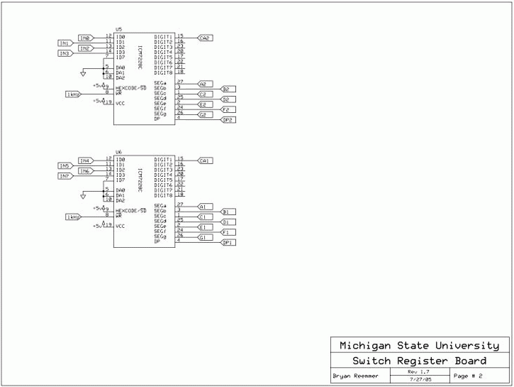
SRB
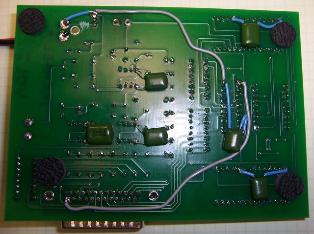
SRB modifications.
The 74LS76 ripple counter project was hampered by failure of the SRB to correctly register inputs. The 7476 ripple counters would get “stuck” at various points of the count, as it attempted to change states but apparently could not build up sufficient voltage. The state machine Lab 5 also saw most students experiencing difficulties–except for the one with the modified SRB.
Students spent extra time rebuilding circuits, swapping ICs, and showing the TA that their circuit was not miswired. The following are possible SRB design issues:
- Inadequate internal power supply voltage: SRB TTL logic may fail to consistently read SRB inputs due to voltage 20% lower than OEM spec’s
- Inadequate IC power filtering: Glitches in SRB operation due to voltage dips through high impedance traces
- No external circuit signaling return: There is no return (“ground”) wire from the external circuit, causing the SRB to act “flaky” e.g. student touches wires and circuit works or doesn’t work
- Shared high impedance power/signal ground/returns: The SRB uses rather thin circuit board traces throughout. The sharing of long, thin traces for power and signaling “ground” can lead to failure to register student circuit inputs properly. Example: SRB “flakes out” at certain points of a 4-bit ripple counter sequence, getting “stuck” on certain numbers of the count.
Design modifications have been implemented on the author’s SRB, which do not fully fix the SRB troubles, but do make it work better.
It is believed that a redesign of the SRB is warranted to provide a better laboratory equipment environment.
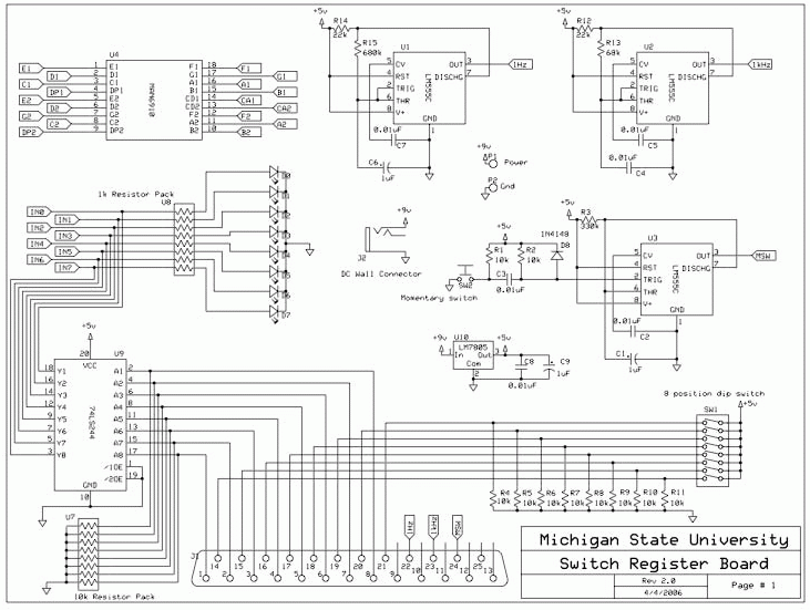
SRB modified schematic.
The SRB (Switch Register Board) is constructed and used by students to interface with their digital logic circuits to provide switch and periodic inputs and visual LED outputs.
The students were only provided with one variable DC power supply. This means that digital logic ICs requiring 5.0 V nominal must share power with the SRB. While the students’ digital logic runs “raw” off of the 5.0 V nominal supply, the SRB has provided an LM7805 fixed 5.0 V regulator.
This throws up a red flag–voltage regulators have considerable internal voltage drop, and prima facie we surmise there will be at least several tenths of a volt voltage drop through the LM7805.
The LM7805 is specified with a minimum input voltage of 7 volts. The LM7805 datasheet calls for a minimum input of 2 volts greater than the desired output. ICs on the SRB are specified with minimum input voltages of 4.75 V. The SRB provides only about 3.8 V when fed with 5.0V input This is as much as 20% outside of IC specifications. This problem exists for the all ICs on the SRB:
- U1, U2, U3: LMC555
- U5, U6: ICM7228CIPI
- U7: 74LS244N
The ICM7228 do not have Vcc input filtering as recommended by the manufacturer and by good engineering practice. The lack of power supply rail filtering leaves the ICM7228 subject to glitches caused by switching transients as LED segments are switched, or other I/O or logic transients are experienced. It would be prudent to provide this filtering for all six ICs on the SRB.
For both analog and digital signaling, a low impedance return path is critical to consistent performance. The SRB has no such return path. The signals must find their return through a daisy-chained power supply arrangement. An independent signaling return path to the SRB from external circuitry should be provided.
Students sometimes experience glitches in circuit operation when wires are touched–even just the insulation of the wire–this may be rectified by proper provisioning of signaling paths. It may be that the other four modifications have helped sufficiently to avoid cutting more traces and soldering more wires on the back of the SRB.
R1 and R2 are incorrectly labeled on the schematic as both 10Kohm resistors. The actual values are: R1: 1.0 Mohm, R2: 100 ohm Reversing the resistors leads to 1/4 Watt dissipation, exceeding the capability of R1 if it is a 1/8 Watt resistor. The “kickback” from the higher load presented with the incorrect wiring may lead to glitches in unfiltered ICs.
SRB Workarounds
To make the Sept 18 2007 ripple counter work, the author did the following:
- Used a second power supply to provide 9 V to the SRB
- Provided an independent signaling return to the SRB
- Removed the pull-down resistors to the 74LS244 in an attempt to further improve signal coupling (this is normally an undesirable configuration, but out of desperation it was tried and helped–other measures should be followed instead as noted above)
This avoids low voltage to SRB ICs causing failure to properly register states. We modify the SRB to have a +5V regulated output to run the external circuit off of. This means you use one power supply set to 9 V, and run your external circuit ONLY off power from the SRB–plugging your external circuit into the 9 V power supply would then overvoltage your external circuit. So run your external circuit off of the SRB only after the modification.
First cut the trace between the unused J2 and the +9 V input (pin 1) of the LM7805 regulator and in place of that trace, run a 18 to 22 gauge wire (hookup wire) between the pad that used to run to the +9 V input of the LM7805 regulator and put the wire to the +5 V output of the LM7805 (pin 3). Then on the J2 pads, solder two flexible stranded 16 gauge wires of a convenient length, say 2 feet, to put banana plugs on. This is what you will run your external circuitry from. Obviously, put a black wire to the pad of J2 that is “ground”, and a red wire to the pad that you soldered the wire to the +5V output to.
Filter IC power sources by adding a 0.1 µF capacitor of tantalum (low ESR) type from V_CC to “ground” on each IC. Do this on the backside of the board, “underneath” each IC. Figure out which pin of the IC is what from the datasheets.
Solder a wire from the unused pin 25 of the SRB DB-25 connector to pin 1 and pin 19 of U7, the 74LS244. This provides a signal return reference point less influenced by the power ground bus. In your logic circuits, always connect from pin 25 of the SRB to the external circuit “ground”. Do not leave this wire as the only ground connection. Always be sure the main black power wire from J2 is also connected to the external circuit.
It is suspected that the 74LS244 voltage glitches are due to high input impedance on its power input. This trace has been wired around and will be tested if possible with an oscilloscope vs. an unmodified SRB.